PCB Layout Services
Microart has been providing PCB Layout Services to Canada and the U.S. for 40 Years.
With the evolution of new technologies and the miniaturization of electronics, PCB's used in all products have become more compact with higher levels of sophistication. Therefore, it becomes more important to do PCB layouts in such a way that they meet the requirements of modern electronic circuits. In order to formulate an effective PCB layout, several layout principles need to be implemented. At Microart Services Inc., we ensure proficient PCB layout utilizing the latest PCB layout techniques and technologies. We provide high-quality Printed Circuit Board layout solutions in adherence to the IPC standards, ensuring the highest reliability, and signal integrity.
Layouts to our customer’s specifications, our highly skilled team is focused on providing quality layouts and prototypes to ensure that your project is completed within a time effective and cost efficient manner. When you choose Microart to engineer your project, we review with you all of your requirements in detail and provide you an opportunity to discuss your plans and ask many questions utilizing our experience and expertise to fully maximize your products potential. We realize that confidentiality is a major concern and will sign an NDA (Non-Disclosure Agreement) enabling us to speak freely about your intimate project details and the different technologies we have to offer you.
Microart’s 4 Layout Rules For Ultimate Manufacturability
The PCB Layout Process at Microart
Schematic Capture
Schematic capture or schematic entry is the first step in the PCB layout & development. The electronic diagram, or electronic schematic of the electronic circuit layout is created by a designer. This is done interactively with the help of CAD Software known as a schematic capture tool or schematic editor. After the completion of the schematic capture process, a completed electronic layout is stored in a file, This file is then converted into a netlist file. The file features inter-connectivity information about component pins or circuit nodes present in the electronic circuit.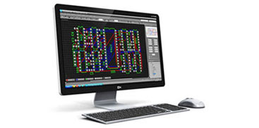
PCB Component Footprint Creation
Component footprint creation helps determine the space available for component placement. A suitable mounting scheme is decided based on component footprint creation. A footprint or land pattern is the arrangement of pads in surface-mount technology (SMT) or through-holes in through-hole technology (THT) used to physically attach and electrically connect a component to a printed circuit board. The footprint creation helps determine the number of layers, which are needed on the board. We can provide PCBs from a single layer up to 30 layers.
Pcb Routing
In PCB design wire routing, is most commonly called routing. The routing step adds wires needed to properly connect the placed components while obeying all design rules for the IC. Our layout designers utilize PCB CAD software to route the physical connections between all the components present on the board. The software makes use of netlist file created earlier from the schematic to route physical connections. Our vast experience and expertise enable us to incorporate simulations and complex routing in PCB layouts.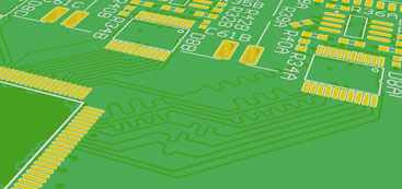
PCB Verification & Analysis
This is an important step in any PCB manufacturing process. To achieve a first pass manufacturable and functioning PCB, it is critical to review the design before proceeding with PCB fabrication. Our skilled PCB designers will, if requested, perform a full design for manufacture rule check. They will not only review the design for routing and footprint verification, but also can check for controlled impedance, line length matching, differential planes, test coverage, proper antenna design, clearance for assembly and many more critical steps to ensure the PCB is correct the first time. Once the Verification is complete, we can also perform functional modeling to verify certain electrical properties are going to function as were meant to. We can then create 3D models of the assembled PCB to aid in the layout of any cases or enclosures that might be required for the final product. When the layout is approved by the customer and signed off, we can then forward a package that will include at least but not limited to the following: • Final Schematic • PCB Design for Manufacture File • Gerbers (OBD++ if requested) • Assembly Drawings • Pick and Place Centroid Data • BOM
At Microart, our PCB layout services are monitored and improved regularly, which ensures providing our customers with excellent PCB layout solutions. To know more about our PCB layout services and PCB layout design for Manufacture, you can always call us on 905.752.0800.
